The accuracy of your sample temperature is key
Cryogenic measurements of devices in conventional cryostats typically require time-consuming and destructive wiring of an on-wafer device. That isn’t the case with cryogenic probe stations. These platforms enable visualization and electrical interrogation of multiple wafer-level devices using positionable probes, accelerating characterization efforts. The tradeoff for optical access to and flexible probing of the device under test lies in the heat loads from thermal radiation and probe arm heat conduction via the probe arms. Because of these loads, as well as the thermal resistance between the device and sample stage, the actual temperature of the device can deviate from the sample stage sensor—leading to inaccurate measurements.
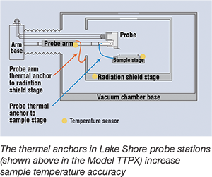
To minimize this effect, the probe station should have radiation shields to reduce the thermal radiation on the sample and the probes should be thermally anchored at or near the sample stage (see the next page for how our stations are designed this way). Below, we examine the role of probe arm thermal anchoring in relationship to device temperature, specifically when attempting to quickly evaluate superconducting circuits, a common application for cryogenic measurements of electronic devices.
Determining conductive heat transfer in a probe station using Cernox® and niobium wire reference measurements
Experimental setup
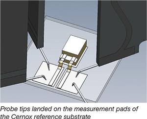
To investigate the role of probe arm thermal anchoring on the device temperature in a cryogenic measurement, a Lake Shore CRX-4K probe station with a fixed 1 W sample stage cooling capacity was chosen as the test platform. For simulating a device under test, a calibrated Cernox® sensor was soldered onto a sapphire substrate, with its underside coated with a thin layer of Apiezon® N grease and clamped to a 32 mm (1.25 in) grounded sample holder. Tungsten tips (25 µm diameter) on four probe arms were landed on the contact pads of the sensor, and the device temperature was obtained with our Model 336 temperature controller using a four-point probing measurement of sensor resistance. Additional temperature sensors within each of the four arms and one bolted to the underside of the sample stage were used to monitor arm and stage temperatures.
Results
Table 1 summarizes the device, stage, and arm temperatures for three common probe arm thermal anchoring configurations. In the recommended configuration, the arm is anchored to the radiation shield and the probe is anchored to the sample stage (as shown in the column to the right). The second configuration relies solely on thermally anchoring both the arm and the probes to the shield, and the final configuration consists of four unanchored arms and the shielding removed.
Table 1—Configuration dependent device temperature
| Probing configuration | Sample stage temp (K) | Mean arm temp (K) | Device temp (K) |
| Arms anchored to radiation shield, probes to sample stage | 4.87 | 9.21 | 7.57 |
| Arms anchored to radiation shield | 3.80 | 34.94 | 12.13 |
| Arms not anchored, no radiation shield | 6.46 | 271.7 | 41.16 |
In the first configuration, the thermal load on the station’s cooling stage is increased by anchoring the probes to the sample stage, resulting in a higher sample stage temperature than in the second configuration with the probes anchored
to the radiation shield. However, the lower sample stage temperature does not translate into a lower device temperature as the extra conductive heat load from the probes is not compensated by the additional cooling through the device substrate. Despite
the relatively small impact on stage temperature by removing the radiation shield and probe/probe arm thermal anchors, the third configuration causes a substantial increase in heat load to the device, driving up the device temperature by more than
30 K.
Discussion
Using well-anchored probes and probe arms, we demonstrate the ability to rapidly evaluate superconducting circuits. For this measurement, a small wire was cut from a 99.8% pure niobium foil (Alfa-Aesar®) and affixed to a sapphire plate with a thin layer of cyanoacrylate adhesive. The wire was then thinned to increase the contrast in resistance between normal and superconducting states; the thinned niobium wire has a 272 mΩ resistance at room temperature. The sapphire substrate was mounted in an identical fashion to the Cernox reference chip, then cooled to cryogenic temperatures in the station. After landing four probes directly on the niobium wire, the wire resistance was monitored as a function of stage temperature with our Model 370 AC resistance bridge equipped with a 3708 pre-amplifier. At each stage temperature setpoint, the system was allowed to stabilize for 5 min prior to acquiring a device resistance.
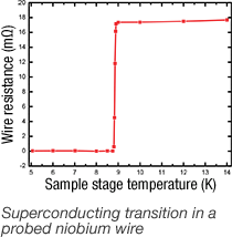
 The figure at left shows the wire resistance as a function of stage temperature, indicating a sharp decrease in the wire resistance at stage temperatures below 8.90 K, which we attribute to the
onset of superconductivity in the probed wire. Below 8.75 K, the wire resistance drops below the measurement accuracy of the experimental setup (<40 µΩ).
Conclusion
By probing a calibrated Cernox sensor and a niobium whisker, we found that conductive heat transfer from the probes can impart a significant thermal load on a device under test, and thermal anchoring is critical for managing the heat transfer and achieving suitable device temperatures. We demonstrated that in a probe station configuration with properly thermally anchored probes and effective radiation shielding, the thermal gradient between device under test and the sample stage can be minimized.
How our stations keep heat from reaching the sample
 Lake Shore’s probe stations take thermal management to the next level, providing a measurement platform you can really trust.
Thermal probe anchoring Lake Shore probe stations include special thermal anchoring to throttle unwanted heat sources. In probe stations without comprehensive thermal anchoring, the device under test may be much warmer than the sample stage itself (and of unknown temperature). Reporting device temperatures based only on a sample stage sensor where heat loads are not controlled can lead to erroneous results. Precise device characterization requires a good understanding of the device’s actual temperature. To avoid injecting unwanted heat into the sample device via the probe arms, the arms and probes must be thermally anchored.
Temperature sensors Lake Shore probes are cooled to the sample stage temperature to minimize heat load to the device under test. Lake Shore sensors on the sample stage, probe arm, and radiation shield provide an accurate thermal profile of the test environment.
Compensating probe Thermal management of the arm means that compensation must also be made at the probe to offset any arm movement during variable temperature experiments. Without a compensating probe, significant ramping of sample stage temperatures may result in contact quality changes during device measurements, possibly shifting the tip enough to leave its contact pad.
Use the Cernox® reference kit to predict accurate sample stage temperature
 Good science demands known experimental conditions. In some cases, sample temperature can vary widely from the set sample stage temperature. The reference Cernox substrate probing kit can take care of that. It has a calibrated Cernox sensor chip mounted to a sapphire substrate with landing pads so that the temperature can be read using four probes. This simulates the thermal loading of a sample during probing, allowing you to accurately measure sample stage temperature. The kit includes necessary adapters and cables to connect either BNC or triaxial probes to a Model 336 input.
Get a new precision current and voltage source—the MeasureReady 155

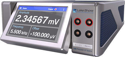
Designed for demanding scientific and engineering applications where a low-noise source of current or voltage is required, This precision current and voltage source provides high-quality excitation for cryogenic probing. The MeasureReady 155 source operates as either a current or voltage source and provides DC and AC output. Exceptional DC noise levels are achieved without external filtering while maintaining bandwidth up to 100 kHz, providing a solid foundation for researchers performing I-V curve, Hall effect, resistance, and other fundamental measurements of novel materials and early-stage devices.
In addition to high-accuracy device testing, the source is particularly ideal for:
- Precision DC I-V and C-V curve measurements of novel materials
- Characterizing new heterostructures where low-noise bias voltages/currents are required
- Providing very low power excitation of sensitive materials like organics
- Controlled characterization of low resistance and superconducting materials

