A new approach to improving confidence in low-level measurements of nanostructures
Introduction
The study of new semiconducting materials, high-temperature superconductors, new photovoltaic devices, and organic electronic materials typically requires low-level sourcing and measurement because the materials are often nanostructures. Types of ultra-small structures include 2-dimensional (2D) nanoelectronic structures, quantum dots, multi-atomic layer heterostructures, and organic semiconductor structures. These extremely small structures are subject to thermal dissipation damage. As device structures get increasingly smaller, these small structures can only tolerate extremely low stimulus currents and voltages, which reduce measurable signals close to the noise floor of typical instrumentation and experimental setups. The resulting measurements needed to fully characterize these structures are, therefore, very low-level signals and thus are often contaminated with significant levels of power line, thermal, and other types of ambient noise signals.
This technical note explores the use of a synchronized and modular AC + DC sourcing and measurement system that utilizes optimum sensitivity, noise rejection, and uninterrupted acquisition of data as a means to more confidently characterize such structures.
Measurement methods and their challenges
Stimulating and making electrical measurements on nanostructures can be performed either with DC techniques or AC techniques extending up to the RF frequency range. Using DC techniques, sensitive and repeatable nV-range measurements can be executed with good precision and repeatability. Additionally, DC measurements can be more accurately traceable to a national standard than an AC measurement. However, DC measurement methods can be susceptible to wide-band noise as well as 1/f or flicker noise, among others. A typical noise distribution is shown in Figure 1. Wide-band or white noise, generated by thermal fluctuations in the measurement apparatus, has a frequency-independent noise power density that extends across the frequency spectrum. Flicker noise is electronic noise generated by flowing current in all passive and active electronic components. It is described as 1/f noise since the noise power density is inversely proportional to the frequency with the highest contribution as the measurement approaches DC or 0 Hz. The frequency around which the dominant noise contribution transitions from flicker noise to wide-band noise is known as the corner frequency and can range from around 50 Hz to over 100 Hz.

Source polarity reversals, multiple measurement steps, and measurement delays to allow settling time can eliminate the thermal offset error. The synchronous AC + DC sourcing and measurement in the M81-SSM can help the user characterize the DC thermal offset error. AC stimulus on a DC bias can eliminate the need for two separate DC voltage measurements to remove a DC thermal offset while simultaneously providing DC bias that may be desirable for sample or device characterization. Additionally, the simultaneous combination of DC and AC measurement can provide more insights into the DUT, and does so more quickly, on computations of resistance, impedance, and harmonic content emanating from a measured signal. DC and AC amplitudes can be swept individually or simultaneously, which increases the information obtained and may also lead to new insights previously not possible to obtain at all or as conveniently.
When electrically characterizing any device or material, some power has to be applied to the DUT to generate a signal, and that power is then dissipated in the DUT as heat. Nanostructures, other extremely thin structures, and single-layer atomic structures have minimal mass and can be easily heated or even destroyed if too much energy is injected into the DUT. Even a semiconductor device that has yet to have a heat sink mounted on the substrate can be easily thermally damaged by the application of a stimulus signal.
Even if the applied energy does not damage the DUT, the added heat can cause a temperature rise in the DUT, and its characteristics that are a function of temperature can change during measurements, producing unwanted or uncontrolled thermal effects.
One option to avoid self-heating-related changes is to require quicker or pulsed measurements so that the DUT will absorb less energy. A pulsed source signal will apply less energy, and high-speed measurement acquisition can allow for a narrow pulse and less average heating. Fast DC measuring with a sampling A/D converter can enable the use of a pulse stimulus. High-speed sampling and the 5 kHz data streaming rate available in the M81-SSM provide continuous observation of the pulsed response and allow additional filtering and noise reduction in a shorter observation time compared with traditional instrumentation.

Figure 1: Conceptual plot of flicker noise (also known as pink noise) and broadband noise (known as white noise). The flicker noise has the 1/f characteristic curve with a corner frequency, FC.
Provided the signal of interest is comparable to or larger than the flicker noise in the system, a DC instrument can achieve a high level of sensitivity by averaging multiple acquisitions. In this way, the bandwidth of the measurements becomes very narrow and limits the impact from the white noise. However, if the 1/f voltage noise is on the order of or even higher than the low-level DC signal, then it is extremely challenging for DC measurement techniques to measure the signal of interest. For this commonly encountered condition in research applications, an AC source and measurement approach can help to extract the signal of interest from the background by moving the measurement frequency away from DC, where the flicker noise contribution is highest.
With this AC method, the material or device under test (DUT) is stimulated by a voltage or current signal at a specific single frequency — referred to as the reference frequency, fref. The signal coming from the measurement then consists of the device noise and modulated DUT response, Asig(2πfsig); DC signals, such as thermoelectric voltages, generated by the apparatus; as well as possible higher order responses that occur at harmonics of the reference frequency.
The modulated signal of interest is typically extracted with a homodyne or lock-in technique. With a modern lock-in amplifier, the compound signal coming from the DUT is digitized and numerically multiplied by a reference sine wave, Arefsin(2πfreft), where Aref is the reference signal amplitude and fref is the reference frequency of the stimulus source. When multiplied by this reference sine wave, any DC signal time averages to 0, while the amplitude of the modulated device response, Asig is derived from a simple trigonometric relation:

Since the primary DUT response should be at the reference stimulus frequency, fref = fsig, then,

Low-pass filters remove the high-frequency component, ½ArefAsig cos(4πfsig), as well as any higher harmonic responses. With the AC lock-in method, as shown in the equations, the output from the homodyne detection is a DC voltage. Any phase shift between the stimulus and response can be determined by multiplying the digitized signal with a phase-shifted reference signal. Provided the stimulus frequency is above the corner frequency, the noise in a lock-in measurement is dominated by white noise. Using longer lock-in time constant selections and a steeper filter slope provided by the lock-in amplifier, the bandwidth of the AC measurement can be adjusted to give the desired signal-to-noise ratio.
A solution: combined DC + AC sourcing and measurement
Recognizing the advantages and disadvantages of DC and AC techniques has traditionally required deciding which types of instrumentation to select and apply. Addressing these challenges, Lake Shore Cryotronics has developed a single instrument offering both DC and AC capabilities and allows each technique, depending on the test environment, to be easily employed, compared, and even combined for the best results. This solution, the MeasureReady™ M81‑SSM synchronous source measure (SSM) system, combines low-level, tightly synchronized DC and AC sourcing and measurement using a half-rack instrument and remote amplifier modules.
The remote amplifier modules employ linear topologies and allow placement close to the material or DUT for minimized susceptibility to noise. One user interface, provided via the half-rack M81 instrument, simplifies the task of controlling and acquiring measurements from multiple amplifier modules. The instrument supervises timing and synchronizes multiple measurements on either a single DUT or multiple DUTs. Figure 2 shows the M81-SSM system, the combination of the instrument and remote amplifiers, when used with a Lake Shore cryogenic probe station, where the DUT would be mounted in the station’s chamber for on-wafer electronic measurements.
Further enhancements minimize the effect of noise
While having both DC and AC sourcing and measurement in one instrument gives the user the flexibility to select the most effective technique for maximum sensitivity, the M81‑SSM offers three additional features that minimize noise. The stimulus signal is a critical element of the test configuration and can be a source of noise. The M81-SSM employs a balanced current source amplifier to minimize common mode noise. In addition, the measurement amplifier has a wide frequency range, enabling the user to operate in a band where noise is low. Furthermore, the amplifier designs minimize internal and external noise sources.
This DC/AC differential current source amplifier employs a balanced circuit topology that enables the DUT to be better isolated from ground and any associated ground loops or noise currents. Essentially, the balanced source presents a differential signal to the DUT and to the associated differential mode-configured measurement amplifier. The floating differential source signal substantially reduces the impact of 50 to 60 Hz common mode noise that can often plague a single-ended current source circuit configuration. An unbalanced single-ended source effectively allows common mode noise to become normal mode noise which a measurement instrument must filter from the actual signal. The balanced current source, with its much greater noise rejection than a single-ended source, is most effective when measuring very low-resistance samples when contained in cryogenic probe stations or cryostats with their associated noise sources.
Unlike a DC measurement system with a narrow range of operation anchored to DC, the M81-SSM modules can operate from very low frequencies (0.1 mHz ) up to 100 kHz. Thus, with the M81 system, the measurement frequency can be selected to avoid 1/f noise and other bands where interference is highest in a test environment. One example is measurement systems with magnetic field drives which often create noise at low-frequency fluctuations below 1 Hz, noise near 50 or 60 Hz line frequencies, as well as interference at higher frequencies up to 100 Hz. In this example, the M81 stimulus source and the phase-sensitive detector could be operated at frequencies outside of these noise bands for optimal measurement performance and efficiency.
The modules are optimized for low-level signals through the use of linear power supplies and purely analog control methods. All digital logic is in the M81 instrument so that there is no digitally generated noise in the source and measurement modules. As shown in Figure 3, the modules can be located close to the DUT. This minimizes noise induced in long signal lines between a conventional instrument and the DUT.
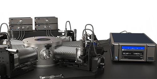
Figure 2. The MeasureReady M81-SSM synchronous source measurement (SSM) system testing in a cryogenic probe station. Shown are voltage source, current source, current measure, and voltage measure modules performing a low-level characterization of an ultra-cold sample under vacuum in a controlled environment.
Patent-pending measurement technique for avoiding the loss of dynamic data
When measuring a fast-changing signal, data is often lost when the signal exceeds the active measurement range. The instrument needs to sense either the overload or underload state and change range. That process takes time, and measurements are lost while the instrument transitions to the new range. The M81-SSM modules use a patent-pending seamless ranging process to avoid interruption of sample capture. The module has two ranges simultaneously active. As the signal approaches the transition between the two ranges, both ranges contribute to the measurement until the signal has moved entirely into the new range. Sampling continues unabated through the range change to avoid any data loss.
Overcoming the challenge of eliminating thermal offset errors and self-heating errors using the M81 Thermal offset voltages exist wherever connections between dissimilar metals exist in a circuit. When characterizing nanomaterials that require low-level stimulus signals, the thermal voltages can be on the order of the measured signal. Figure 3 shows a test configuration in which the thermal voltage error is modeled as a lumped element, DC voltage. Also, applying power to a nanomaterial can easily cause the material to heat up, potentially causing changes in its characteristics.
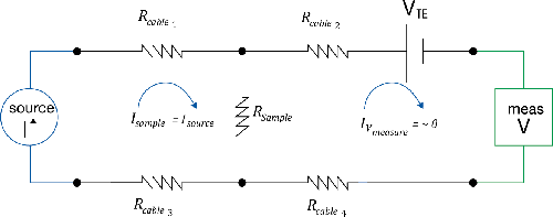
Figure 3. A thermal voltage error modeled as a DC voltage source. Thermal voltage errors are significant sources of measurement error when making low-level measurements.
A second option is to use phase-sensitive detection so that a lower stimulus current or voltage can be applied to the DUT to minimize the energy applied, and the phase-sensitive detector can extract lower-level signals from the interfering noise and background noise. Using AC stimulus and phase-sensitive detection can also accomplish the objective of minimizing the applied energy, similar to pulsed DC methods. AC methods can give acceptable results using less averaging, which reduces the total number of measurements. Fewer measurements combined with a lower stimulus signal minimizes thermal effects. Having both DC sourcing and measurement as well as AC sourcing and measurement capability, along with analog/digital filtering and averaging options, provides added flexibility for minimizing DUT parametric variations due to self-heating.
Characterizing a structure’s small signal and large signal performance in a single test
Another example of the advantages of combination synchronous DC and AC sourcing and measurement is demonstrated in the simultaneous characterization of a nonlinear device’s large and small signal performance. An AC signal superimposed on a varying DC bias can generate the parameters to directly measure differential conductance, as shown in Figure 4. The DC bias can characterize the large signal performance of the non-linear device separately or at the same time the AC characteristics are measured, which may expose DC-level non-linearities and other second-order effects of interest.
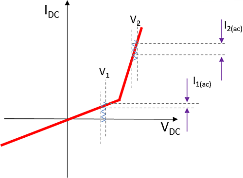
Figure 4. The combination of AC and DC sourcing and measuring enables characterization of a nonlinear device’s small signal and large signal performance using one stimulus sweep for differential conductance applications.
Gaining confidence in test data
When conducting original research, validating test results builds confidence in conclusions based on the data. For studies that involve low-level signals, the researcher will want to validate results with multiple samples to gain confidence in the data. With conventional instrumentation, tests on each DUT must be performed sequentially due to limited channel capabilities and other setup limitations. Sequential testing also adds additional variables, such as slight changes in the environment over time. In addition, results from the instrumentation used can also be susceptible to variations in temperature or in humidity over the test time interval. Furthermore, when each new sample or device is connected to the test system, changes in connection impedances add another variable that impacts repeatability and reduces confidence in the results.
The M81-SSM system allows testing up to three DUTs in parallel with one test setup. All sourcing and measurement channels are sampled at precisely the same time. The synchronization of the source outputs and the measurements improves consistency and repeatability and ensures that the DUTs are simultaneously tested under exactly the same test conditions. All measurements are triggered simultaneously at a continuous rate of 2.6 µs. Testing multiple samples at once speeds up data collection and validates data. A three-DUT test setup of the synchronous sourcing and measuring system is shown in Figure 5.
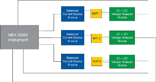
Figure 5. Block diagram of the M81-SMM system characterizing three DUTs at the same time. The DUTs could be nanowires or carbon nanotubes, or any resistive samples or devices. Some types of DUTs can be connected in series, which would allow the use of a single current source amplifier, enabling a more cost-effective setup and with the added benefit of identical current flow in each series connected device to eliminate a possible error source.
A summary of performance advantages with the M81-SSM synchronous source measure system
Superior rejection of noise with:
- The capability of making DC and AC measurements to either measure in a very narrow, very low-frequency bandwidth or to extract low-level signals from noise at a selected frequency
- Operation over the programmable frequency range of 0.1 mHz to 100 kHz
- Remote analog sourcing and measurement amplifier modules that can be placed close to a DUT for minimizing noise pickup and interference from test cabling
- Absence of digital signal generation in the remote amplifier modules that eliminates noise from sharp-edged clock and data lines
- A balanced current source and differential voltage measurement, which maximizes 50/60 Hz common mode noise rejection
- Programmable averaging for DC measurements and programmable time constant settings for the AC phase‑sensitive detection measurements to maximize signal-to-noise performance
AC + DC sourcing and measurement that is tightly synchronized to enable the capture of more high-quality data in the least amount of time so one can:
- Obtain AC small signal measurements and DC large-signal measurements in a single sweep
- Perform DC and AC measurements without disturbing a sample and risking changes in connection impedances or damaging a fragile sample
- Use 375 kHz sampling to capture dynamic signals and to reduce measurement time, which minimizes errors due to DUT self-heating
- Use seamless range changing to allow continuous observation of a signal even when the signal has changes over orders of magnitude
- Obtain time-stamped data with intervals as short as 2.6 µs for synchronization of stimulus-response studies and for testing multiple DUTs under identical conditions
- Extract harmonics which is essential for impedance spectroscopy applications
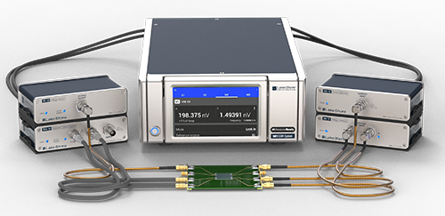
Modular configuration allows a wide range of tests with one M81 instrument and multiple configurations of remote modules.
Operation with one control interface for the multiple source and measurement functions, which:
- Simplifies the instrument setup learning curve because only one instrument interface has to be learned
- Simplifies synchronization of instruments because all timing and control come from one instrument
- Eliminates communication, hardware, and data flow between instruments because one instrument performs all timing, control, and signal processing
- Simplifies data transfer to a computer because all data come from a single instrument
Conclusion
All these capabilities combined make the M81-SSM synchronous source measure (SSM) system a superior solution for characterizing nanostructures, single- and multilayer atomic structures, MEMs, quantum structures, and organic semiconductors. The M81-SSM is an excellent choice for any type of low-level or I/V measurements.

